Master Project (PDM) · 2026
Quantitative Characterisation of SiPM Radiation Damage using Emission Microscopy
Overview
Silicon Photomultipliers (SiPMs) are the photodetector of choice for the LHCb Scintillating-Fibre (SciFi) tracker and are increasingly ubiquitous across high energy physics. Their principal weakness is the dark count rate (DCR) — a light-independent noise floor that grows with the neutron fluence accumulated in the collider environment, and which will become a limiting factor for the High-Luminosity LHC (HL-LHC) and the LHCb Upgrade II. Understanding where inside each microcell the radiation damage sits, and how strongly each defect contributes to the noise, is essential for qualifying and developing radiation-tolerant sensors.
This project applies Emission Microscopy (EMMI) — a defect-localisation method borrowed from semiconductor failure analysis — to directly image the faint infrared light emitted by dark-count avalanches in SiPMs from two manufacturers, FBK (W3m, 31 µm pitch, Vbd ≈ 31 V) and Hamamatsu (H2024, 50 µm pitch, Vbd ≈ 51 V), each studied with a non-irradiated reference and four neutron fluences up to 1×10¹³ neq/cm² — three times the dose the SciFi SiPMs are expected to accumulate over the full HL-LHC programme. A reproducible Python pipeline turns these images into quantitative, cell-level observables, reconstructing individual emission hotspots as 2D Gaussians and following their number, brightness, size, current contribution and in-cell position as a function of over-voltage and fluence.
Headline result: the total emission intensity is strictly proportional to the dark current, independent of neutron fluence, so EMMI is a faithful spatial proxy for DCR. On top of this, the pipeline extracts per-hotspot damage statistics and reveals that radiation-induced hotspots cluster in a characteristic square ring inside each cell — establishing emission microscopy as a cell-level diagnostic for SiPMs in future high-radiation detectors.
Why It Matters: SiPMs at the LHCb Upgrade II
In the LHCb SciFi tracker, SiPM arrays are coupled directly to the ends of the scintillating fibres and read out the light produced by traversing charged particles. Their radiation tolerance therefore sets a hard limit on the operational lifetime of the tracker. The forthcoming LHCb Upgrade II will raise the integrated luminosity by roughly a factor of five, and with it the radiation fluence seen by the detectors.
The SiPMs sit away from the beam axis, in a region of reduced but still significant neutron flux. FLUKA simulations of the detector indicate that, integrated over the full programme, the SciFi SiPMs will accumulate approximately 3×10¹² neq/cm². This study characterises damage up to 1×10¹³ neq/cm² — a comfortable three-fold safety margin — with the goal of building a diagnostic that helps develop and qualify the next generation of radiation-hard SiPMs.
How a SiPM Works
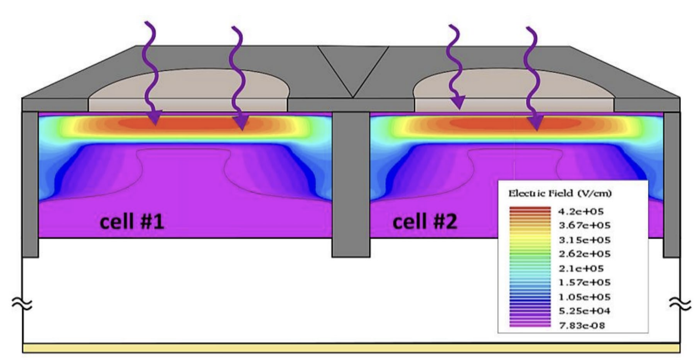
A SiPM is a dense two-dimensional array of Single-Photon Avalanche Diodes (SPADs), or microcells, each a reverse-biased p–n junction operated in Geiger mode — biased above its breakdown voltage Vbd. The amount by which the bias exceeds breakdown is the over-voltage (OV = Vbias − Vbd), which sets the gain and trigger probability. When a free charge carrier — from an absorbed photon or a thermal fluctuation — enters the high-field region, the field is strong enough to develop a self-sustaining avalanche through impact ionisation. A quenching resistor then stops the avalanche and the cell recharges with a recovery time τrec = RqCcell.
Because every fired cell delivers essentially the same charge, and the cell outputs are summed, the SiPM signal is proportional to the number of cells fired, giving photon-counting capability. Compared with the vacuum photomultiplier tubes traditionally used in HEP, SiPMs are compact, offer high granularity, are insensitive to magnetic fields and operate at low bias — but they are vulnerable to radiation damage.
Dark Count Rate — the Damage Proxy
The dominant intrinsic noise of a SiPM is the spontaneous, light-independent firing of microcells: the dark count rate. Its microscopic origin lies in lattice defects. In a perfect crystal, promoting an electron across the full silicon bandgap (Eg ≈ 1.12 eV) is strongly suppressed at the operating temperature. Defects — whether from manufacturing or, crucially here, from radiation-induced displacement damage — create mid-gap energy levels that act as stepping stones: through the Shockley–Read–Hall (SRH) mechanism a carrier is thermally excited to a trap and then to the conduction band in two smaller steps, dramatically enhancing the generation rate. A carrier generated this way inside the high-field region triggers an avalanche electrically indistinguishable from a genuine photon count.
Because each defect provides a generation centre, the DCR scales with the density of mid-gap states and therefore rises monotonically with accumulated fluence. This direct correspondence between lattice defects and dark counts is exactly what makes the spatial distribution of dark-count activity a proxy for the distribution of radiation damage — the map that emission microscopy produces. The DCR also depends on temperature (∝ exp(−Ea/kT)), over-voltage, and pixel size; under irradiation, traps additionally act as trap-assisted-tunnelling centres, which dominate at the reduced temperatures used to run irradiated detectors.
Secondary Photon Emission
Charge-carrier multiplication in the high-field region is accompanied by faint light emission — roughly one photon for every 10⁵–10⁶ carriers. It is this secondary emission that EMMI detects and uses as an optical signature of avalanche (and hence dark-count) activity. Three processes contribute, visible on the silicon band structure:
- Intraband bremsstrahlung: hot carriers accelerated by the field decelerate by emitting photons without changing band, giving a broad visible-to-infrared continuum (~500–1600 nm). This is the primary source of the observed emission.
- Indirect interband recombination: phonon-assisted electron–hole recombination near the gap, giving near-infrared emission (~1100–1200 nm) at very low efficiency, but measurable given the ~10⁵–10⁶ carriers per avalanche.
- Direct interband recombination: quasi-direct transitions at the Γ-point (~3.4 eV, UV ~365 nm), mostly reabsorbed within the silicon before escaping.
Experimental Setup
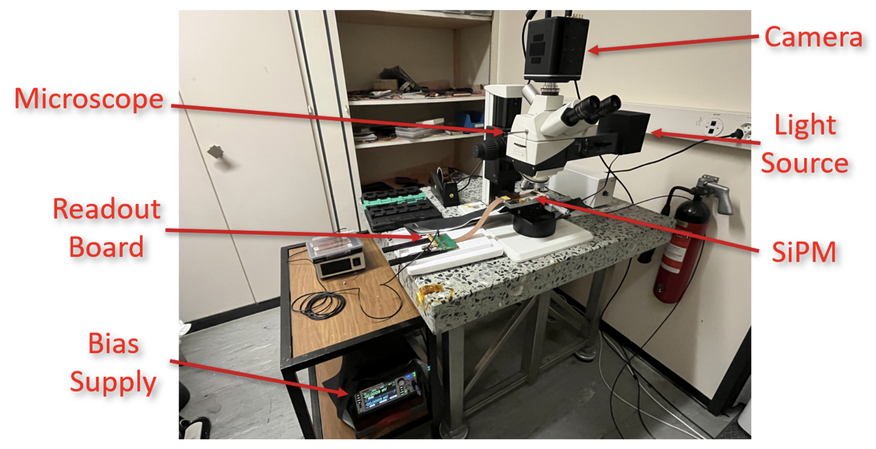
Measurements were carried out on an emission-microscopy bench in the dark room of the Cubotron building at EPFL. The imaging sensor is a Hamamatsu ORCA-Quest 2 qCMOS camera (C15550-22UP), cooled to −20 °C and read out at 16-bit over a 4096×2304 frame. Each SiPM is held flat on a vacuum chuck under a Leica microscope (5×/20×/50× objectives) and biased through a Keithley 2450 SourceMeter, which simultaneously logs the leakage current every 5 seconds. A halogen lamp provides brief illumination for the reference image only; a black cloth blocks stray light from the camera LED and power supply during the long emission exposures.
The EMMI Technique
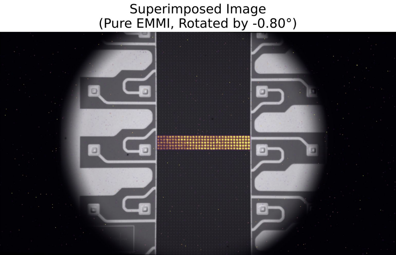
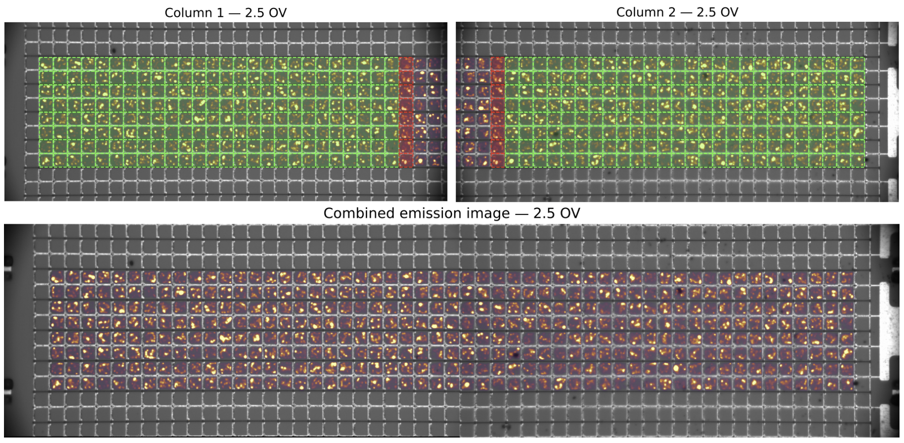
Emission microscopy superimposes two images to localise where light is emitted inside the sensor:
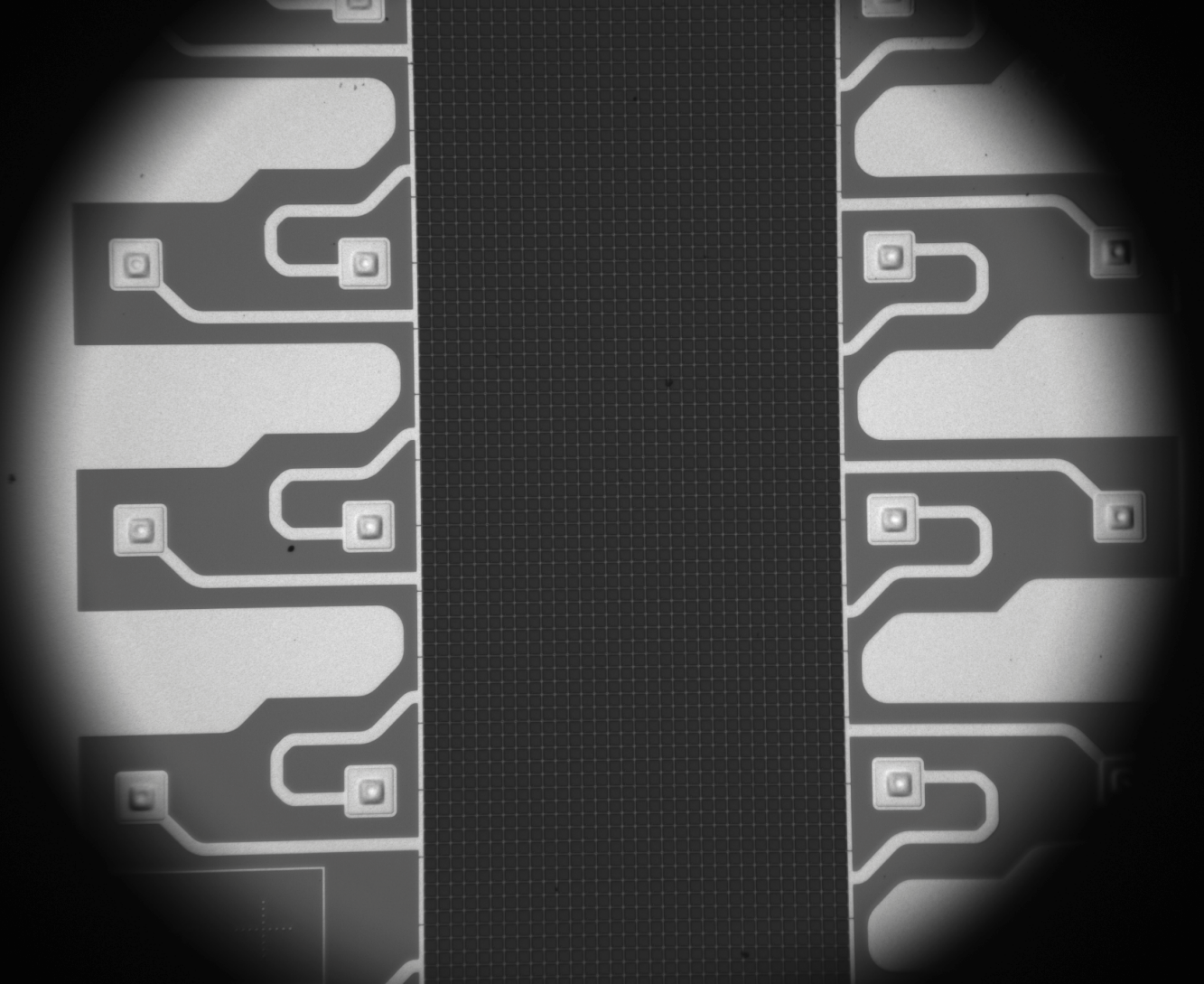
- Reference image — a short (~3 ms) illuminated exposure recording the microcell grid structure.
- Emission image — a 10-minute exposure in complete darkness, recording only the secondary photons from avalanches at a chosen over-voltage.
The two are co-registered and overlaid using a customised "plasma" colormap in which the pixel value is coupled to the opacity channel, so that dim pixels render transparent and only genuine emission stands out against the reference. First developed for integrated-circuit failure analysis in the 1990s, EMMI is here transferred to SiPMs — allowing radiation damage to be studied cell by cell rather than only as a bulk current.

Devices Under Study
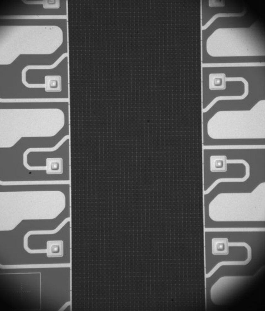
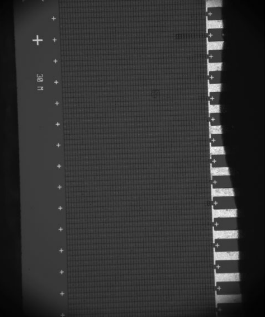
Two SiPM technologies were studied, each across a non-irradiated reference plus four neutron fluences — ten samples in total. The Hamamatsu H2024 has 128 channels of 5 rows × 32 columns of 50 µm cells (160 cells per channel); the FBK W3m has 128 channels of 8 rows × 55 columns of 31 µm cells, of which the two end columns are inactive, leaving 424 active cells per channel. Breakdown voltages, extracted with the ILD method below, are stable to within ~0.2 V across fluence for each manufacturer, confirming that irradiation shifts the dark-count rate rather than the breakdown point.
Hamamatsu H2024 (50 µm pitch)
| Name | Pixel Size | Fluence (neq/cm²) | Vbd ch118 |
|---|---|---|---|
| H2024 | 50 µm | 1×10¹³ | 51.69 ± 0.02 V |
| H2024 | 50 µm | 3×10¹² | 50.97 ± 0.02 V |
| H2024 | 50 µm | 1×10¹² | 51.45 ± 0.07 V |
| H2024 | 50 µm | 3×10¹¹ | 51.31 ± 0.02 V |
| H2024 | 50 µm | 0 (reference) | 51.10 ± 0.11 V |
FBK W3m / W1m (31 µm pitch)
| Name | Pixel Size | Fluence (neq/cm²) | Vbd ch118 |
|---|---|---|---|
| W3m | 31 µm | 1×10¹³ | 31.07 ± 0.02 V |
| W3m | 31 µm | 3×10¹² | 31.00 ± 0.02 V |
| W3m | 31 µm | 1×10¹² | 31.11 ± 0.02 V |
| W3m | 31 µm | 3×10¹¹ | 31.19 ± 0.02 V |
| W1m | 31 µm | 0 (reference) | 30.94 ± 0.04 V |
Breakdown Voltage — the ILD Method
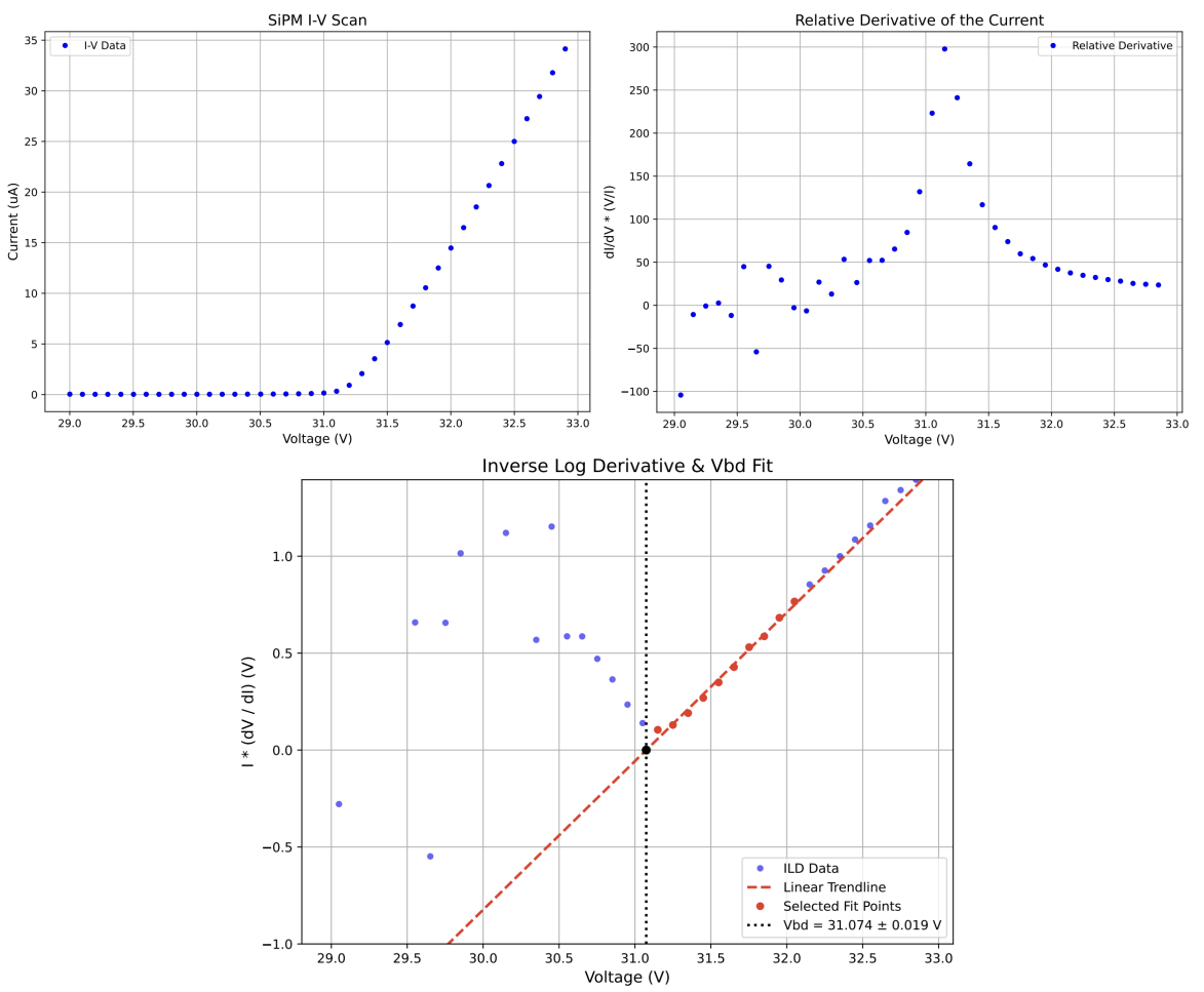
The breakdown voltage of each channel is extracted with the Inverse Logarithmic Derivative (ILD) method. Just above breakdown the SiPM current follows a power law in over-voltage, I(V) ∝ (V − Vbd)1+κ, so the ILD — the inverse of the relative logarithmic derivative, (dI/dV)·(V/I), multiplied by V — varies linearly with bias and extrapolates to zero at V = Vbd. A linear fit to the region above breakdown therefore gives a precise Vbd at the voltage intercept. For the non-irradiated sensors, whose dark current is very small, the measurement is instead performed under illumination.
From Raw Frames to Per-Cell Data
Turning the 10-minute exposures into quantitative, cell-level numbers requires a multi-stage image-processing pipeline, developed in Python (NumPy / SciPy / scikit-image).
1. Camera noise subtraction
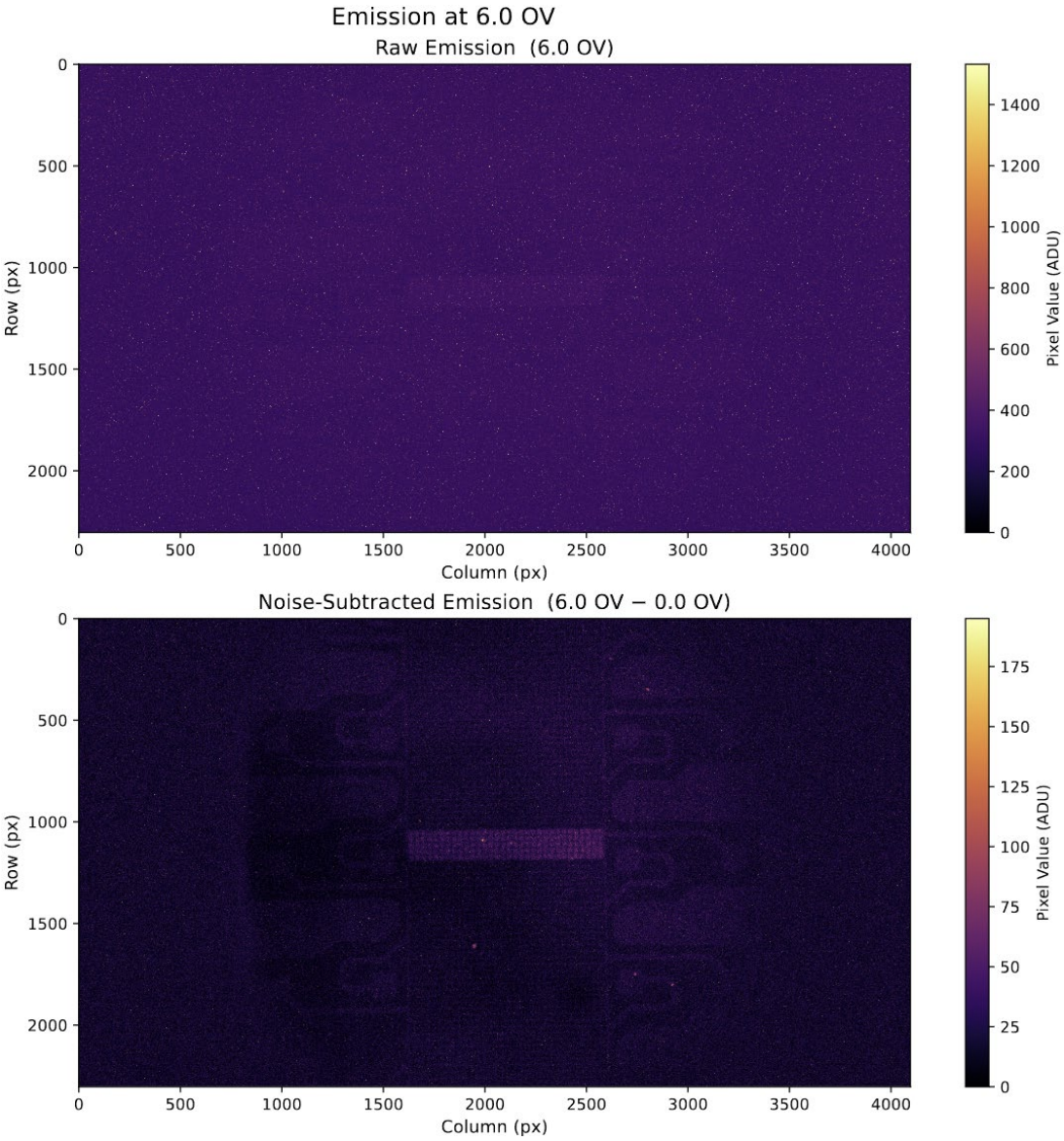
The qCMOS sensor contains persistently bright pixels from manufacturing defects (fixed-pattern noise). A dark frame of equal 10-minute exposure, taken with no bias applied, is subtracted pixel-wise from every emission image. The markedly cleaner result validates the fixed-additive-offset assumption and reveals the underlying cell structure and genuine emission.
2. Grid identification & channel merging
The image is first rotated so that the variance of the column-summed brightness profile is maximised, aligning the cell walls with the pixel axes. The rows and columns of extreme brightness are then located as cell borders — bright strips for the Hamamatsu sensors, dark strips for the FBK ones. The residual misalignment (~2 px) is negligible against the ~10 px cell-wall thickness. Because the 20× objective images only half a channel at a time, the two halves are acquired separately and stitched into the complete channel.
3. Hotspot extraction as 2D Gaussians
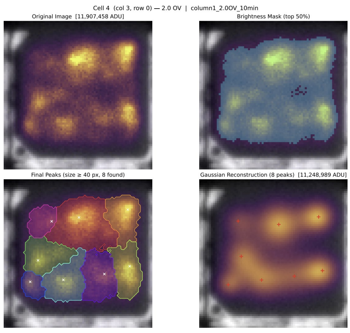
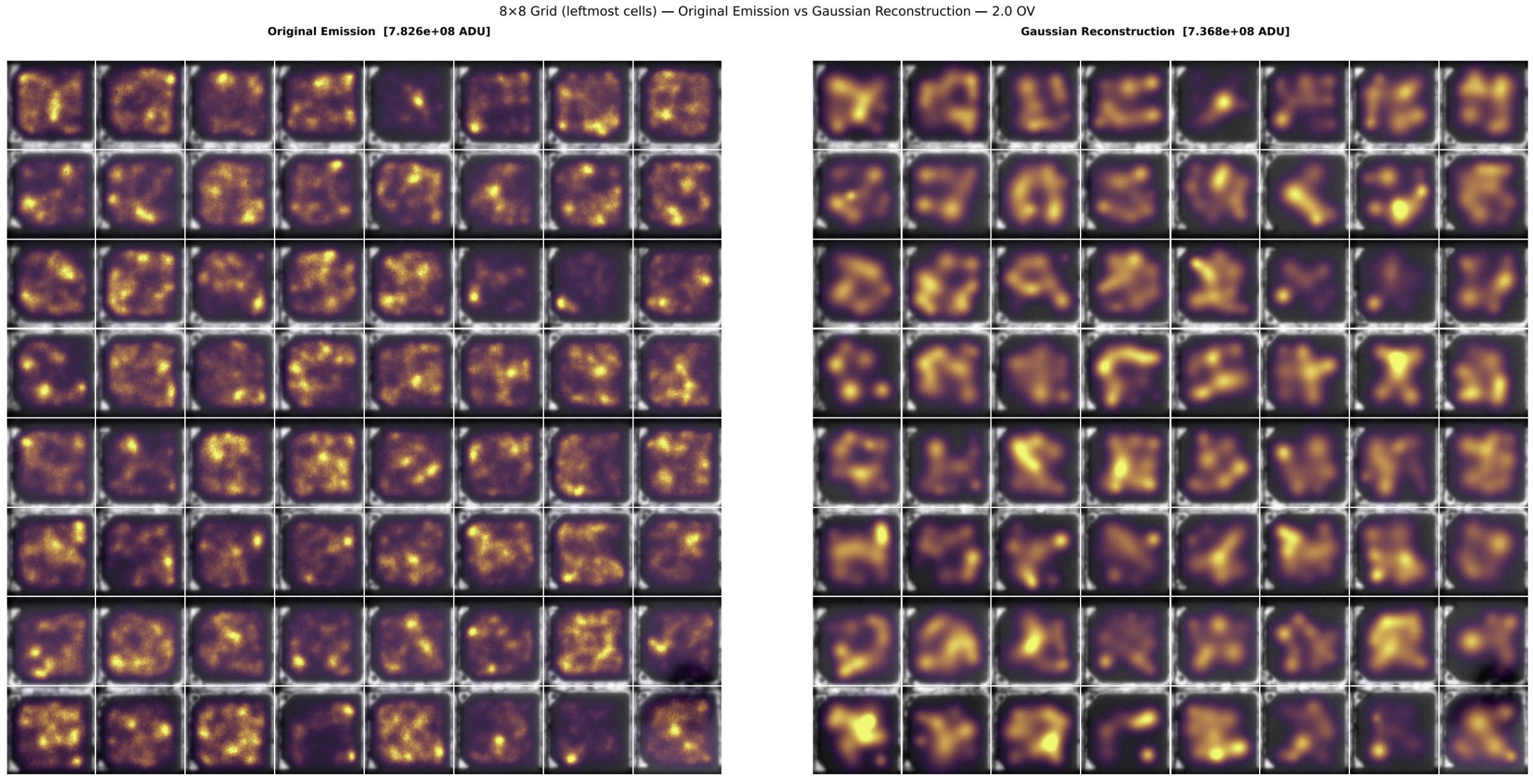
Within each cell, the emission hotspots are reconstructed as 2D Gaussians in three steps: an adaptive percentile threshold builds an active-pixel mask (robust even for dim hotspots at low OV); peak_local_max followed by watershed segmentation assigns each above-threshold pixel to a peak; and each peak is converted into a 2D Gaussian whose location is the intensity-weighted mean, amplitude the mean of the three brightest pixels, and width area-matched to the peak. A global rescale corrects for overlapping-Gaussian double-counting, at the cost of a known ~5% amplitude bias.
Result 1 — Dark I–V vs. Fluence
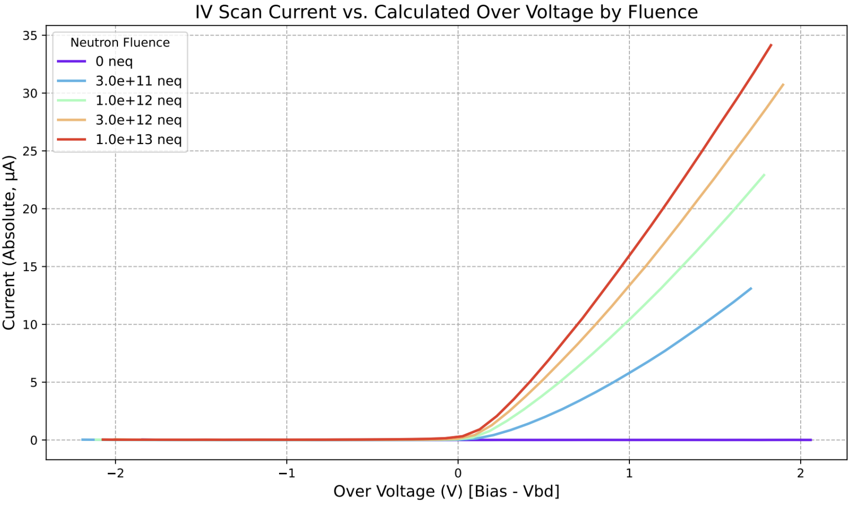
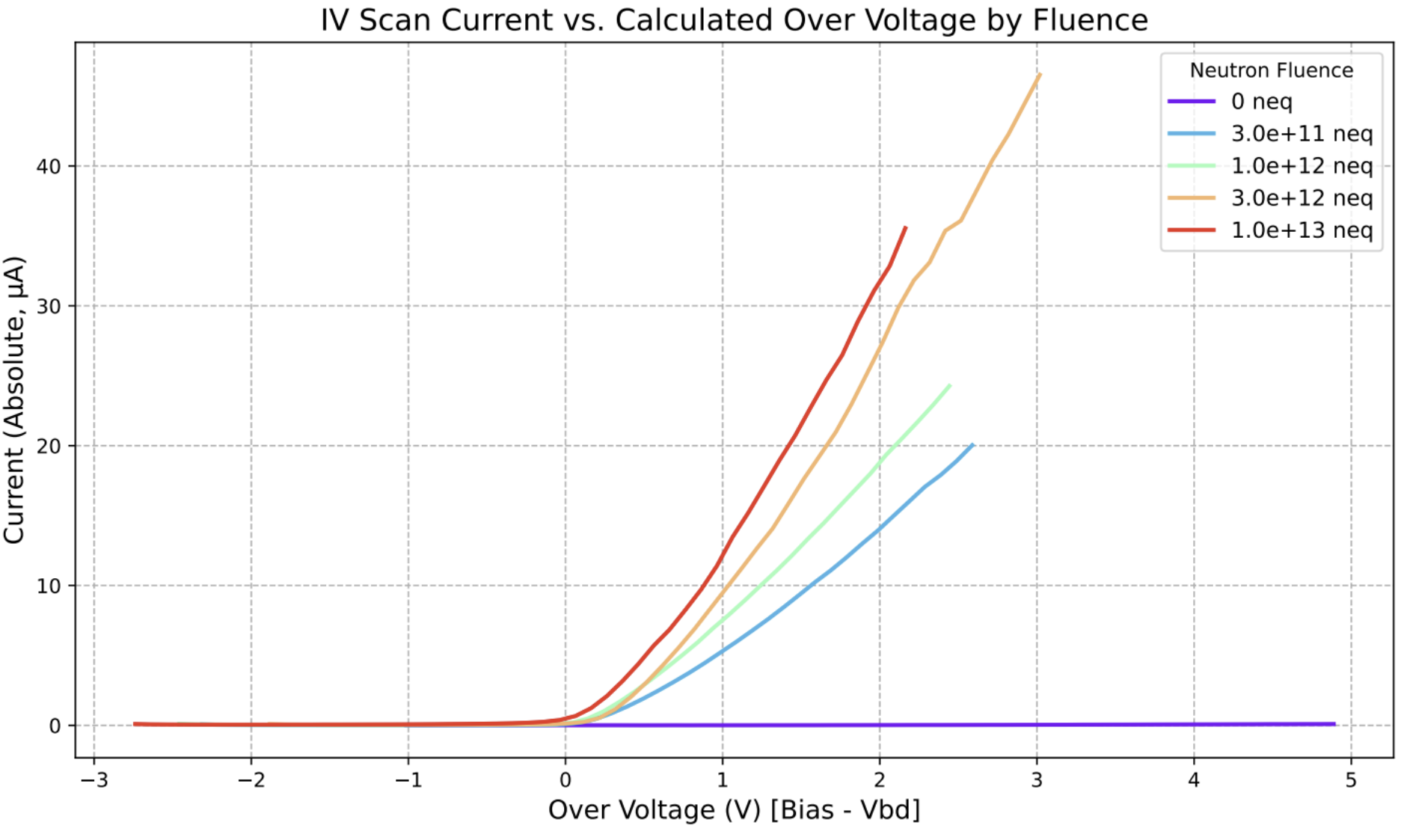
The dark current at a fixed over-voltage rises with fluence, as expected from the increasing density of generation centres — but the rise is sub-linear. In the unsaturated regime each avalanche releases the full gain charge and the current should be linear in fluence; the compression at high fluence is the signature of recovery-time saturation, where cells re-fire before the field has fully recharged over τrec. The practical consequence is that the effective over-voltage seen by a heavily irradiated cell is lower than the nominal applied value — a caution to keep in mind when comparing quantities across fluences at fixed nominal OV.
Result 2 — Per-Cell Emission Intensity
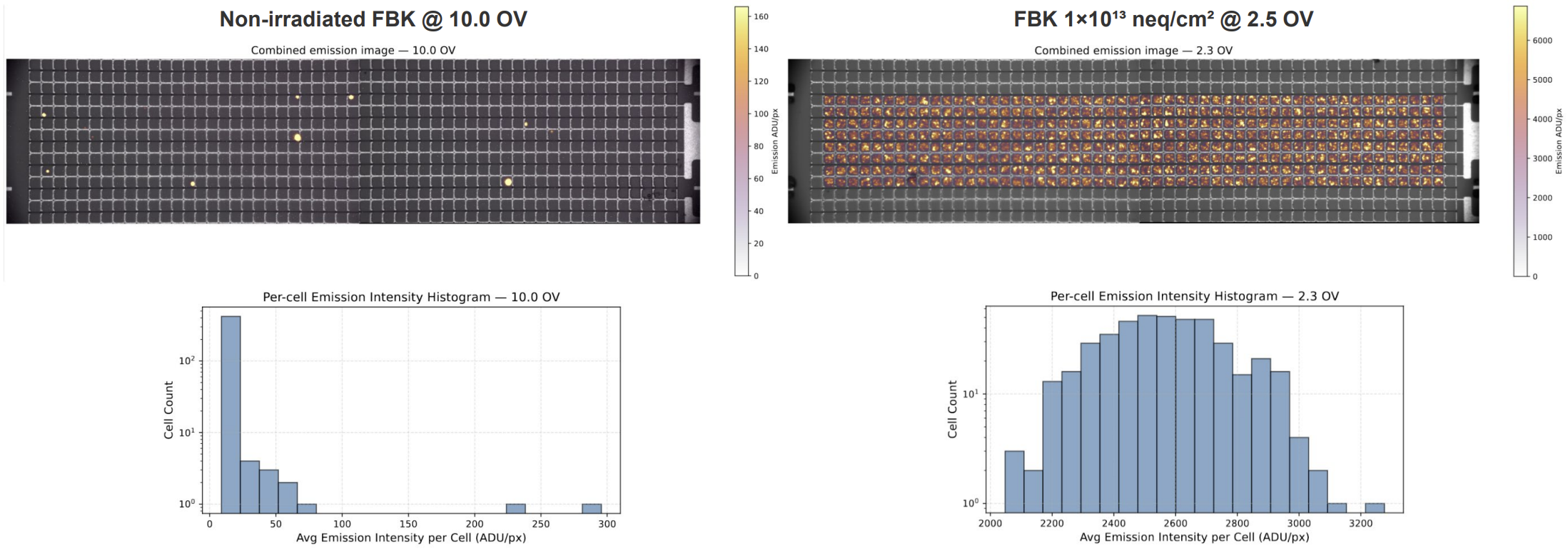
Averaging the emission over each cell gives a useful first-order observable. For the non-irradiated FBK sensor at 10.0 OV, two cells stand out as 4–5× brighter than the rest — the optical signature of isolated manufacturing defects, appearing as clear outliers above an otherwise narrow distribution. After irradiation this contrast is washed out: the uniform neutron exposure introduces bulk damage everywhere, so the per-cell histogram collapses to a single peak with no outliers.
Result 3 — Emission Intensity ∝ Dark Current
Plotting the averaged emission intensity against the simultaneously measured dark current, for every bias point and fluence, yields a single universal straight line for each manufacturer — the emitted light tracks the total avalanche charge irrespective of how the damage that produced it was distributed. The FBK slope, 2.82×10⁴ photons/µC, is steeper than the Hamamatsu 1.92×10⁴ photons/µC, indicating more photons emitted per unit charge in the finer-pitched device.
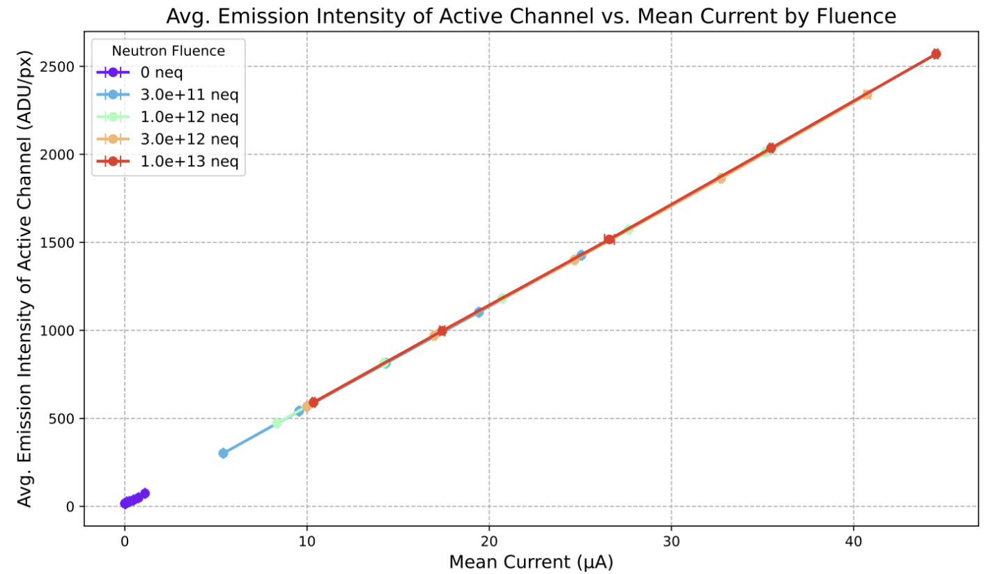
Key finding: emission intensity is strictly proportional to dark current, independent of neutron fluence from 0 to 1×10¹³ neq/cm². Emission microscopy is therefore a faithful spatial proxy for DCR across the full range of radiation damage studied.
Result 4 — Photons Produced per Charge Carrier
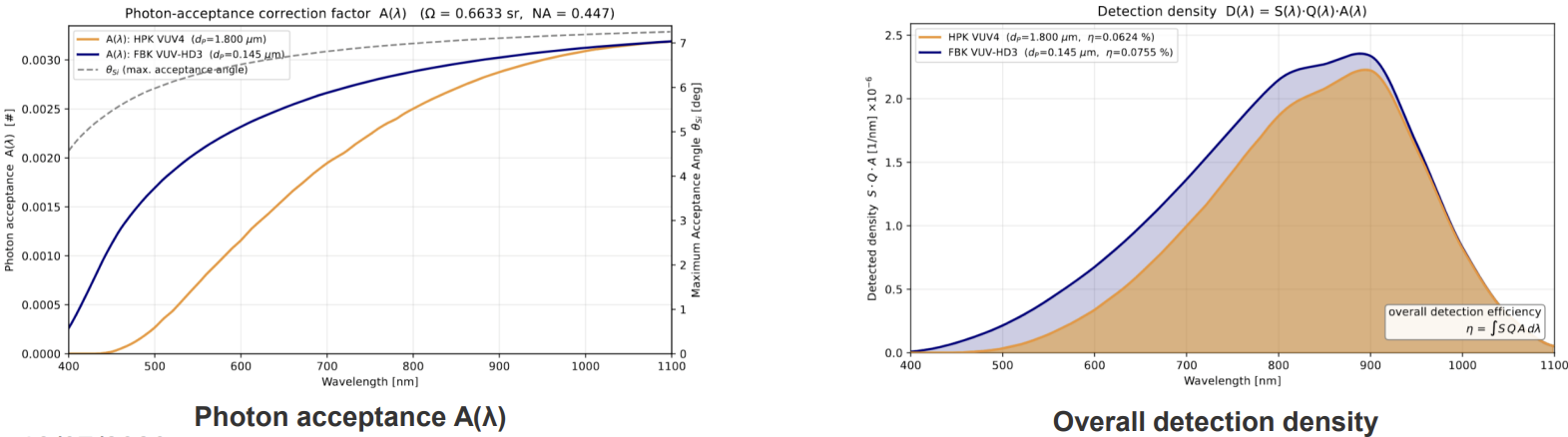
The measured slopes give the number of photons detected per charge carrier; converting to the number produced requires correcting for the full optical chain. This combines the camera quantum efficiency (from the manufacturer), the SiPM emission spectrum (adopted from McLaughlin et al., for want of a spectrometer), and a wavelength-dependent photon-acceptance correction factor A(λ) that folds together the geometric acceptance of the 20× objective, slant-path attenuation in silicon, and Fresnel reflection losses at the Si/SiO₂ and SiO₂/air interfaces via Snell's law.
Integrating the resulting detection density over wavelength gives overall detection efficiencies of 0.076% (FBK) and 0.062% (Hamamatsu), and hence 5.98×10⁻⁶ and 4.92×10⁻⁶ photons produced per charge carrier. These reproduce the order of magnitude of the literature value (~5×10⁻⁶ for FBK, ~9×10⁻⁶ for Hamamatsu) despite the setup limitations, supporting the validity of the method. The higher FBK yield is consistent with its smaller, more densely packed cells sustaining a stronger local field and hence hotter carriers.
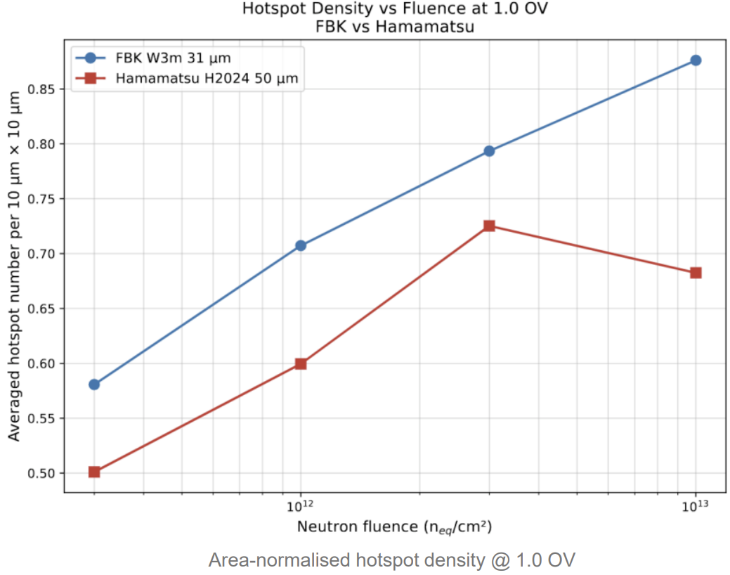
Result 5 — Hotspot Density
Reconstructing individual hotspots allows their number per cell to be counted. At fixed fluence the count is roughly constant with over-voltage — as expected, since the number of damage sites is set by the irradiation, not the operating field — with a slight decrease at high OV as neighbouring hotspots brighten and merge. Normalising by cell area to compare the two pitches, the finer FBK cells show a systematically higher hotspot density, rising monotonically from ~0.58 to ~0.88 hotspots per (10 µm)² with fluence. The Hamamatsu density turns over slightly at the highest fluence (~0.73 → ~0.68) as its numerous bright hotspots merge — an algorithmic resolution limit rather than a genuine loss of damage sites.
Result 6 — Hotspot Brightness, Size & Current
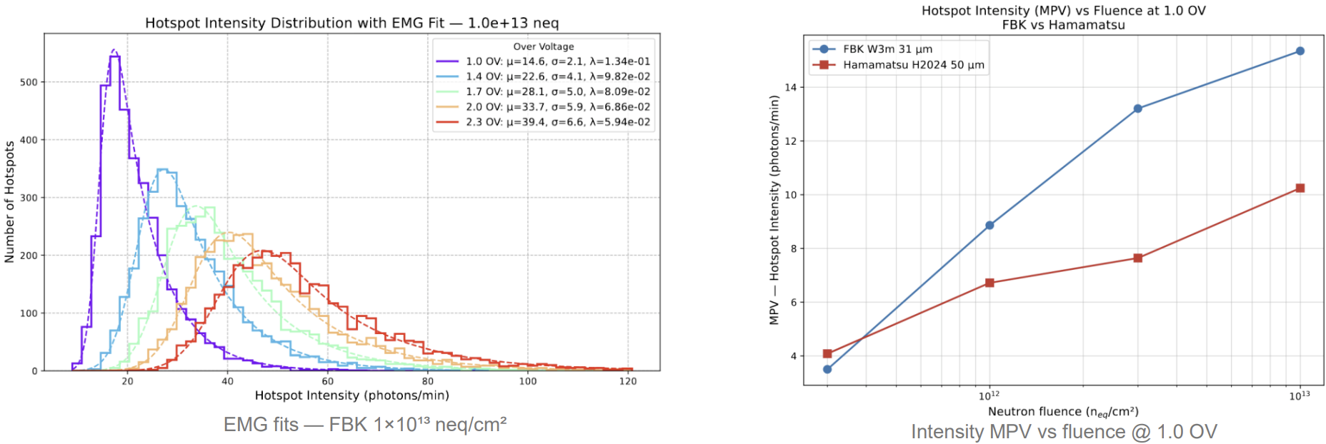
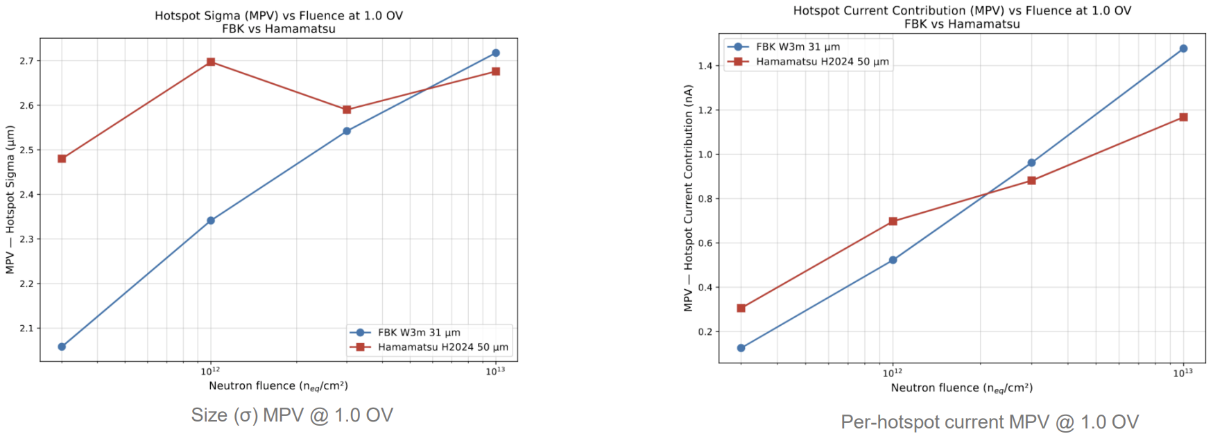
The distributions of per-hotspot intensity, spatial size (σ) and current contribution are each well described by an Exponentially Modified Gaussian (EMG) — a Gaussian bulk of typical hotspots plus a long positive tail from the brightest damage sites — across all over-voltages and fluences. The most-probable value (MPV) of each fit then serves as a single damage metric, and its growth with fluence makes it a candidate for inferring the accumulated dose non-destructively.
- Intensity: the two manufacturers agree at low fluence (~4 photons/min), but FBK rises more steeply, reaching ~15 vs. ~10 photons/min at 1×10¹³ neq/cm².
- Size: the ordering is opposite — the larger Hamamatsu cells give bigger hotspots at low fluence (~2.5 vs. ~2.1 µm), but FBK grows steadily while Hamamatsu stays roughly constant, so the two converge to ~2.7 µm.
- Current contribution: combining brightness and size, both rise from ~0.1–0.3 nA to ~1.2–1.5 nA and cross near 3×10¹² neq/cm², where the steeper FBK growth overtakes Hamamatsu.
Result 7 — Where the Damage Sits: the Square Ring
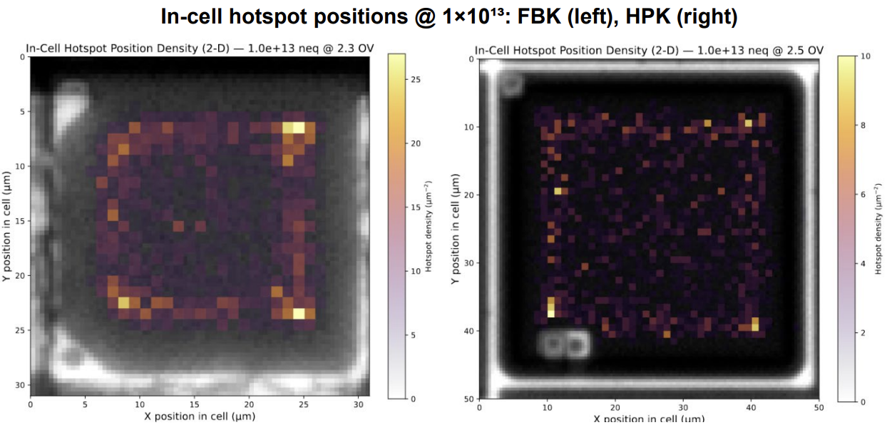
In the non-irradiated sensors the few hotspots gather at the cell borders, consistent with manufacturing defects and the strong edge fields that develop at high over-voltage. In the irradiated sensors, the intensity-weighted centres of the hotspots cluster neither at the cell centre nor at the extreme edges, but in a distinctive square ring set in from the borders — a pattern that shows up as a double-peaked structure in the 1D projections and, most clearly, as a bright square ring in the 2D in-cell position histogram.
The most likely cause is the extent of the depletion region, which lies above the multiplication volume and carries a field strong enough to drift carriers but too weak to trigger avalanches. Neutron-generated carriers there drift into the high-field volume and trigger avalanches at its perimeter — exactly the observed ring. The amplitude of the hotspots around the ring shows no strong positional bias, indicating the ring marks where avalanches are triggered rather than where emission is strongest. Since the cell corners appear especially vulnerable, round-shaped cells could potentially mitigate this effect.
Result 8 — Fill-Factor Estimation
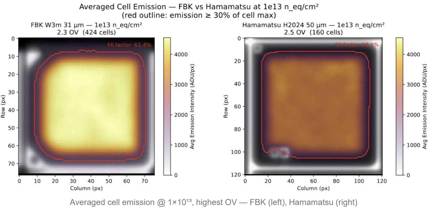
Because the light-emitting regions are exactly those with a field strong enough to sustain an avalanche, the fill factor can be estimated from the fraction of the cell area that emits. Using the averaged cell emission at the highest fluence and over-voltage, and defining the active area as the contiguous region emitting more than 30% of the peak intensity, gives fill factors of 61.4% (FBK) and 58.9% (Hamamatsu). The finer-pitched FBK device is slightly ahead, consistent with the smaller dead-area fraction expected for a finer cell pitch. These should be read as lower bounds, since carriers drifting in from the depletion region make the effective photosensitive area somewhat larger than the light-emitting area measured here.
Summary & Outlook
Emission ∝ dark current, independent of fluence: EMMI is a direct spatial probe of DCR from 0 to 1×10¹³ neq/cm². After correcting the full optical chain, the photon-production yields (5.98×10⁻⁶ FBK, 4.92×10⁻⁶ Hamamatsu per charge carrier) are consistent with the literature.
Cell-level damage statistics: the watershed → 2D-Gaussian pipeline extracts per-hotspot number, brightness, size and current contribution, all well described by Exponentially Modified Gaussian fits whose MPVs grow with fluence — candidate non-destructive metrics for inferring the accumulated dose.
The square ring: radiation-induced hotspots cluster in a square ring inside each cell, consistent with carriers drifting from the depletion region into the multiplication volume. The vulnerability of the cell corners suggests round-shaped cells as a possible mitigation.
The main limitation is the hand-tuned hotspot-extraction algorithm, whose peak-separation parameter can bias the count where hotspots merge; a systematic figure of merit for the reconstruction quality, together with simultaneous multi-Gaussian fitting, would allow these parameters to be optimised and the residual ~5% amplitude bias removed. The natural next step is to calibrate the hotspot-intensity MPV against fluence, turning EMMI into a quantitative, cell-level diagnostic for screening radiation-hard SiPM candidates and cross-checking simulated damage maps.
This work forms part of a broader effort at LPHE, EPFL to understand and mitigate radiation damage in SiPMs destined for the LHCb Upgrade II, and, more broadly, to establish a diagnostic that remains applicable in the even harsher radiation environments of future experiments.
All Research